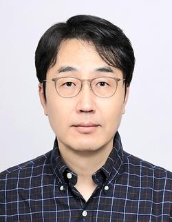
- 조수행 Cho Soohaeng
-
- Campus : MIRAE Campus
- Department : Department of Physics and Engineering Physics
- E-mail : SHCHO@YONSEI.AC.KR
- Tel : 033-760-2868
- Office : Changjo-gwan 224 ho
-
Educational Background
Ph. D., Electrical Engineering
University of Colorado • Boulder, Colorado, USA • August 2002
Dissertation: <111>-Oriented (In,Ga)As/(Al,Ga)As Quantum Well Structures and their Optical and Strain-induced Piezoelectric and Pyroelectric Properties
M. S., Physics
Yonsei University • Seoul, South Korea • February 1995
Thesis: A Mössbauer Study of Nix(Cu0.5Fe0.5)1-XCr2S4
B. S., Physics
Yonsei University • Seoul, South Korea • February 1993
Experience
=== Research Staff
Semiconductor device laboratory • Samsung Advanced Institute of Technology • Yongin-Si, Gyeonggi-Do, Korea • September 2003 to February 2009
• Working on a board-level optical interconnection
• Participated on a development project of high power 650nm red laser diode project for the application of DVD/RW and a Blue/Green frequency doubled Vertical External Cavity Surface Emitting Laser development project for laser TV and large area projection display applications
• Lead a measurement and analysis team.
• Design and characterize laser structures.
• Develop the detailed knowledge of Research & Business Development (R&BD) and mass production processes.
=== Research Assistant + 1 Yr. Postdoctoral research associate
University of Colorado • Boulder, Colorado, USA • September 1996 to August 2003 (graduated in August 2002)
• Evaluated optical, material, structural, piezoelectric, and pyroelectric properties of QW and QW laser structures with strained InGaAs layers grown on (111) and (100) GaAs substrates.
• Hands-on experience on OMVPE growth, doping profile measurements, and wafer preparation of compound semiconductor optoelectronic structures.
• Experimentally determined the pyroelectric coefficient of strained InGaAs layers for the first time to the best of my knowledge.
• Performed the characterization of QW interfaces using various optical techniques, i.e. photoluminescence, photoreflectance, contactless electroreflectance, photocurrent, and differential photocurrent and compared the measurements to transmission electron microscopy and high-resolution X-ray diffractometry.
=== Visiting Researcher
E.T.S.I.Telecomunicación – U.P.M. • Madrid, Spain • January 1999 to February 1999
• Performed differential photocurrent spectroscopy and device fabrication processes, and trained coworkers to analyze the differential photocurrent spectra.
=== Full Time Teaching Assistant
Yonsei University • Seoul, South Korea • March 1995 to May 1996
• Supervised the intermediate and advanced physics experimental laboratory classes and maintained the experimental equipments.
=== Teaching Assistant and Research Assistant
Yonsei University • Seoul, South Korea • March 1993 to February 1995
• Studied the Mössbauer spectroscopy of magnetic compound materials.
• Designed and automated the computerized data acquisition system.
• Supervised various physics laboratory classes.
Research Interest
• Electronic materials and devices
- Flexible and transparent conducting materials and devices
- Non-volatile resistive-switching memory
• Optoelectronic materials and devices
- Laser, LED, Solar cell
- Flexible and transparent conducting materials and devices
- Non-volatile resistive-switching memory
• Optoelectronic materials and devices
- Laser, LED, Solar cell
